


The model of computation provided by an ordinary computer assumes that the basic arithmetic operations--addition, subtraction, multiplication, and division--can be performed in constant time. This abstraction is reasonable, since most basic operations on a random-access machine have similar costs. When it comes to designing the circuitry that implements these operations, however, we soon discover that performance depends on the magnitudes of the numbers being operated on. For example, we all learned in grade school how to add two natural numbers, expressed as n-digit decimal numbers, in
This chapter introduces circuits that perform arithmetic functions. With serial processes,
We start in Section 29.1 by presenting combinational circuits. We shall see how the depth of a circuit corresponds to its "running time." The full adder, which is a building block of most of the circuits in this chapter, serves as our first example of a combinational circuit. Section 29.2 presents two combinational circuits for addition: the ripple-carry adder, which works in
Like the comparison networks of Chapter 28, combinational circuits operate in parallel: many elements can compute values simultaneously as a single step. In this section, we define combinational circuits and investigate how larger combinational circuits can be built up from elementary gates.
Arithmetic circuits in real computers are built from combinational elements that are interconnected by wires. A combinational element is any circuit element that has a constant number of inputs and outputs and that performs a well-defined function. Some of the elements we shall deal with in this chapter are boolean combinational elements--their inputs and outputs are all drawn from the set {0,1}, where 0 represents FALSE and 1 represents TRUE.
A boolean combinational element that computes a simple boolean function is called a logic gate. Figure 29.1 shows the four basic logic gates that will serve as combinational elements in this chapter: the NOT gate (or inverter), the AND gate, the OR gate, and the XOR gate. (It also shows two other logic gates--the NAND gate and the NOR gate--that are required by some of the exercises.) The NOT gate takes a single binary input x, whose value is either 0 or 1, and produces a binary output z whose value is opposite that of the input value. Each of the other three gates takes two binary inputs x and y and produces a single binary output z.
The operation of each gate, and of any boolean combinational element, can be described by a truth table, shown under each gate in Figure 29.1. A truth table gives the outputs of the combinational element for each possible setting of the inputs. For example, the truth table for the XOR gate tells us that when the inputs are x = 0 and y = 1, the output value is z = 1; it computes the "exclusive OR" of its two inputs. We use the symbols
Combinational elements in real circuits do not operate instantaneously. Once the input values entering a combinational element settle, or become stable--that is, hold steady for a long enough time--the element's output value is guaranteed to become both stable and correct a fixed amount of time later. We call this time differential the propagation delay of the element. We assume in this chapter that all combinational elements have constant propagation delay.
A combinational circuit consists of one or more combinational elements interconnected in an acyclic fashion. The interconnections are called wires. A wire can connect the output of one element to the input of another, thereby providing the output value of the first element as an input value of the second. Although a single wire may have no more than one combinational-element output connected to it, it can feed several element inputs. The number of element inputs fed by a wire is called the fan-out of the wire. If no element output is connected to a wire, the wire is a circuit input, accepting input values from an external source. If no element input is connected to a wire, the wire is a circuit output, providing the results of the circuit's computation to the outside world. (An internal wire can also fan out to a circuit output.) Combinational circuits contain no cycles and have no memory elements (such as the registers described in Section 29.4).
As an example, Figure 29.2 shows a combinational circuit, called a full adder, that takes as input three bits x, y, and z. It outputs two bits, s and c, according to the following truth table:
Output s is the parity of the input bits,
and output c is the majority of the input bits,
(In general, the parity and majority functions can take any number of input bits. The parity is 1 if and only if an odd number of the inputs are 1's. The majority is 1 if and only if more than half the inputs are 1's.) Note that the c and s bits, taken together, give the sum of x, y, and z. For example, if x = 1, y = 0, and z = 1, then
1For clarity, we omit the commas between sequence elements when they are bits.
Each of the inputs x, y, and z to the full adder has a fan-out of 3. When the operation performed by a combinational element is commutative and associative with respect to its inputs (such as the functions AND, OR, and XOR), we call the number of inputs the fan-in of the element. Although the fan-in of each gate in Figure 29.2 is 2, we could redraw the full adder to replace XOR gates A and E by a single 3-input XOR gate and OR gates F and G by a single 3-input OR gate.
To examine how the full adder operates, assume that each gate operates in unit time. Figure 29.2(a) shows a set of inputs that becomes stable at time 0. Gates A-D, and no other gates, have all their input values stable at that time and therefore produce the values shown in Figure 29.2(b) at time 1. Note that gates A-D operate in parallel. Gates E and F, but not gate G, have stable inputs at time 1 and produce the values shown in Figure 29.2(c) at time 2. The output of gate E is bit s, and so the s output from the full adder is ready at time 2. The c output is not yet ready, however. Gate G finally has stable inputs at time 2, and it produces the c output shown in Figure 29.2(d) at time 3.
As in the case of the comparison networks discussed in Chapter 28, we measure the propagation delay of a combinational circuit in terms of the largest number of combinational elements on any path from the inputs to the outputs. Specifically, we define the depth of a circuit, which corresponds to its worst-case "running time," inductively in terms of the depths of its constituent wires. The depth of an input wire is 0. If a combinational element has inputs x1, x2, . . . ,xn at depths d1, d2, . . . ,dn respectively, then its outputs have depth max{d1, d2, . . . ,dn} + 1. The depth of a combinational element is the depth of its outputs. The depth of a combinational circuit is the maximum depth of any combinational element. Since we prohibit combinational circuits from containing cycles, the various notions of depth are well defined.
If each combinational element takes constant time to compute its output values, then the worst-case propagation delay through a combinational circuit is proportional to its depth. Figure 29.2 shows the depth of each gate in the full adder. Since the gate with the largest depth is gate G, the full adder itself has depth 3, which is proportional to the worst-case time it takes for the circuit to perform its function.
A combinational circuit can sometimes compute faster than its depth. Suppose that a large subcircuit feeds into one input of a 2-input AND gate but that the other input of the AND gate has value 0. The output of the gate will then be 0, independent of the input from the large subcircuit. In general, however, we cannot count on specific inputs being applied to the circuit, and the abstraction of depth as the "running time" of the circuit is therefore quite reasonable.
Besides circuit depth, there is another resource that we typically wish to minimize when designing circuits. The size of a combinational circuit is the number of combinational elements it contains. Intuitively, circuit size corresponds to the memory space used by an algorithm. The full adder of Figure 29.2 has size 7, for example, since it uses 7 gates.
This definition of circuit size is not particularly useful for small circuits. After all, since a full adder has a constant number of inputs and outputs and computes a well-defined function, it satisfies the definition of a combinational element. A full adder built from a single full-adder combinational element therefore has size 1. In fact, according to this definition, any combinational element has size 1.
The definition of circuit size is intended to apply to families of circuits that compute similar functions. For example, we shall soon see an addition circuit that takes two n-bit inputs. We are really not talking about a single circuit here, but rather a family of circuits--one for each size of input. In this context, the definition of circuit size makes good sense. It allows us to define convenient circuit elements without affecting the size of any implementation of the circuit by more than a constant factor. Of course, in practice, measurements of size are much more complicated, involving not only the choice of combinational elements, but also concerns such as the area the circuit requires when integrated on a silicon chip.
29.1-1
In Figure 29.2, change input y to a 1. Show the resulting value carried on each wire.
29.1-2
Show how to construct an n-input parity circuit with n - 1 XOR gates and depth
29.1-3
Show that any boolean combinational element can be constructed from a constant number of AND, OR, and NOT gates. (Hint: Implement the truth table for the element.)
29.1-4
Show that any boolean function can be constructed entirely out of NAND gates.
29.1-5
Construct a combinational circuit that performs the exclusive-or function using only four 2-input NAND gates.
29.1-6
Let C be an n-input, n-output combinational circuit of depth d. If two copies of C are connected, with the outputs of one feeding directly into the inputs of the other, what is the maximum possible depth of this tandem circuit? What is the minimum possible depth?
We now investigate the problem of adding numbers represented in binary. We present three combinational circuits for this problem. First, we look at ripple-carry addition, which can add two n-bit numbers in
We start with the ordinary method of summing binary numbers. We assume that a nonnegative integer a is represented in binary by a sequence of n bits
Given two n-bit numbers a =
Observe that each sum bit si is the parity of bits ai, bi, and ci (see equation (29.1)). Moreover, the carry-out bit ci+1 is the majority of ai, bi, and ci (see equation (29.2)). Thus, each stage of the addition can be performed by a full adder.
An n-bit ripple-carry adder is formed by cascading n full adders FA0, FA1, . . . , FAn-1, feeding the carry-out ci+1 of FAi directly into the carry-in input of FAi+1. Figure 29.4 shows an 8-bit ripple-carry adder. The carry bits "ripple" from right to left. The carry-in c0 to full adder FA1 is hardwired to 0, that is, it is 0 no matter what values the other inputs take on. The output is the (n+1)-bit number s =
Because the carry bits ripple through all n full adders, the time required by an n-bit ripple-carry adder is
Ripple-carry addition requires
The key observation is that in ripple-carry addition, for i
As an example, let ai-1 = bi-1. Since the carry-out ci is the majority function, we have ci = ai-1 = bi-1 regardless of the carry-in ci-1. If ai-1 = bi-1 = 0, we can kill the carry-out ci by forcing it to 0 without waiting for the value of ci-1 to be computed. Likewise, if ai-1 = bi-1 = 1, we can generate the carry-out ci = 1, irrespective of the value of ci-1.
If ai-1
Figure 29.5 summarizes these relationships in terms of carry statuses, where k is "carry kill," g is "carry generate," and p is "carry propagate."
Consider two consecutive full adders FAi-1 and FAi together as a combined unit. The carry-in to the unit is ci-1, and the carry-out is ci+1. We can view the combined unit as killing, generating, or propagating carries, much as for a single full adder. The combined unit kills its carry if FAi kills its carry or if FAi-1 kills its carry and FAi propagates it. Similarly, the combined unit generates a carry if FAi generates a carry or if FAi-1 generates a carry and FAi propagates it. The combined unit propagates the carry, setting ci+1 = ci-1, if both full adders propagate carries. The table in Figure 29.6 summarizes how carry statuses are combined when full adders are juxtaposed. We can view this table as the definition of the carry-status operator
We can use the carry-status operator to express each carry bit ci in terms of the inputs. We start by defining x0 = k and
for i = 1, 2, . . . , n. Thus, for i = 1, 2, . . . , n, the value of xi is the carry status given by Figure 29.5.
The carry-out ci of a given full adder FAi-1 can depend on the carry status of every full adder FAj for j = 0, 1, . . . , i - 1. Let us define y0 = x0 = k and
for i = 1, 2, . . . , n. We can think of yi as a "prefix" of x0
Lemma 29.1
Define x0, x1, . . . , xn and y0, y1, . . . , yn by equations (29.3) and (29.4). For i = 0, 1, . . . ,n, the following conditions hold:
1. yi = k implies ci = 0,
2. yi = g implies ci = 1, and
3. yi = p does not occur.
Proof The proof is by induction on i. For the basis, i = 0. We have y0 = x0 = k by definition, and also c0 = 0. For the inductive step, assume that the lemma holds for i - 1. There are three cases depending on the value of yi.
1. If yi = k, then since yi = yi-1
2. If yi = g, then either we have xi = g or we have xi = p and yi-1 = g. If xi = g, then ai-1 = bi-1= 1, which implies ci = 1. If xi = p and yi-1 = g, then ai-1
3. If yi = p, then Figure 29.6 implies that yi-1 = p, which contradicts the inductive hypothesis.
Lemma 29.1 implies that we can compute each carry bit ci by computing each carry status yi. Once we have all the carry bits, we can compute the entire sum in
By using a prefix circuit that operates in parallel, as opposed to a ripple-carry circuit that produces its outputs one by one, we can compute all n carry statuses y0, y1, . . . , yn more quickly. Specifically, we shall design a parallel prefix circuit with O(lg n) depth. The circuit has
Before constructing the parallel prefix circuit, we introduce a notation that will aid our understanding of how the circuit operates. For integers i and j in the range 0
Thus, for i = 0, 1, . . . , n, we have [i, i] = xi, since the composition of just one carry status xi is itself. For i, j, and k satisfying 0
since the carry-status operator is associative. The goal of a prefix computation, in terms of this notation, is to compute yi = [0, i] for i= 0, 1, . . . , n.
The only combinational element used in the parallel prefix circuit is a circuit that computes the
The two
Some time after this upward phase of computation, the node receives from its parent the product [0, i - 1] of all inputs that come before the leftmost input xi that it spans. The node now likewise computes values for its children. The leftmost input spanned by the node's left child is also xi, and so it passes the value [0, i - 1] to the left child unchanged. The leftmost input spanned by its right child is xj, and so it must produce [0, j - 1]. Since the node receives the value [0, i - 1] from its parent and the value [i, j - 1] from its left child, it simply computes [0, j - 1]
Figure 29.9 shows the resulting circuit, including the boundary case that arises at the root. The value x0 = [0, 0] is provided as input at the root, and one more
If n is an exact power of 2, then the parallel prefix circuit uses 2n - 1
Now that we have a parallel prefix circuit, we can complete the description of the carry-lookahead adder. Figure 29.10 shows the construction. An n-bit carry-lookahead adder consists of n + 1 KPG boxes, each of
A carry-lookahead adder can add two n-bit numbers in O(lg n) time. Perhaps surprisingly, adding three n-bit numbers takes only a constant additional amount of time. The trick is to reduce the problem of adding three numbers to the problem of adding just two numbers.
Given three n-bit numbers x =
As shown in Figure 29.11 (a), it does this by computing
for i = 0, 1, . . . , n - 1. Bit v0 always equals 0.
The n-bit carry-save adder shown in Figure 29.11(b) consists of n full adders FA0, FA1, . . . , FAn - 1. For i = 0, 1, . . . , n - 1, full adder FAi takes inputs xi, yi, and zi. The sum-bit output of FAi is taken as ui, and the carry-out of FAi is taken as vi+1. Bit v0 is hardwired to 0.
Since the computations of all 2n + 1 output bits are independent, they can be performed in parallel. Thus, a carry-save adder operates in
29.2-1
Let a =
29.2-2
Prove that the carry-status operator
29.2-3
Show by example how to construct an O(lg n)-time parallel prefix circuit for values of n that are not exact powers of 2 by drawing a parallel prefix circuit for n = 11. Characterize the performance of parallel prefix circuits built in the shape of arbitrary binary trees.
29.2-4
Show the gate-level construction of the box KPGi. Assume that each output xi is represented by
29.2-5
Label each wire in the parallel prefix circuit of Figure 29.9(a) with its depth. A critical path in a circuit is a path with the largest number of combinational elements on any path from inputs to outputs. Identify the critical path in Figure 29.9(a), and show that its length is O(lg n). Show that some node has
29.2-6
Give a recursive block diagram of the circuit in Figure 29.12 for any number n of inputs that is an exact power of 2. Argue on the basis of your block diagram that the circuit indeed performs a prefix computation. Show that the depth of the circuit is
29.2-7
What is the maximum fan-out of any wire in the carry-lookahead adder? Show that addition can still be performed in O(lg n) time by a
29.2-8
A tally circuit has n binary inputs and m =
29.2-9
Show that n-bit addition can be accomplished with a combinational circuit of depth 4 and size polynomial in n if AND and OR gates are allowed arbitrarily high fan-in. (Optional: Achieve depth 3.)
29.2-10
Suppose that two random n-bit numbers are added with a ripple-carry adder, where each bit is independently 0 or 1 with equal probability. Show that with probability at least 1 - 1/n, no carry propagates farther than O(1g n) consecutive stages. In other words, although the depth of the ripple-carry adder is
The "grade-school" multiplication algorithm in Figure 29.13 can compute the 2n-bit product p =
Each term m(i) is called a partial product. There are n partial products to sum, with bits in positions 0 to 2n - 2. The carry-out from the highest bit yields the final bit in position 2n - 1.
In this section, we examine two circuits for multiplying two n-bit numbers. Array multipliers operate in
An array multiplier consists conceptually of three parts. The first part forms the partial products. The second sums the partial products using carry-save adders. Finally, the third sums the two numbers resulting from the carry-save additions using either a ripple-carry or carry-lookahead adder.
Figure 29.14 shows an array multiplier for two input numbers a =
Let us examine the construction of the array multiplier more closely. Given the two input numbers a =
Since the product of 1-bit values can be computed directly with an AND gate, all the bits of the partial products (except those known to be 0, which need not be explicitly computed) can be produced in one step using n2 AND gates.
Figure 29.15 illustrates how the array multiplier performs the carry-save additions when summing the partial products in Figure 29.13. It starts by carry-save adding m(0), m(1), and 0, yielding an (n + 1)-bit number u(1) and an (n + 1)-bit number v(1). (The number v(1) has only n + 1 bits, not n + 2, because the (n + 1)st bits of both 0 and m(0) are 0.) Thus, m(0) + m(1) = u(1) + v(1). It then carry-save adds u(1), v(1), and m(2), yielding an (n + 2)-bit number u(2) and an (n + 2)-bit number v(2). (Again, v(2) has only n + 2 bits because both
In fact, the carry-save additions in Figure 29.15 operate on more bits than strictly necessary. Observe that for i = 1, 2, . . . , n - 1 and j = 0, 1, . . . , i - 1, we have
Let us now examine the correspondence between the array multiplier and the repeated carry-save addition scheme. Each AND gate is labeled by
Except for the full adders in the top row (that is, for i = 2, 3, . . . , n - 1), each full adder
Finally, let us examine the output of the array multiplier. As we observed above,
Data ripple through an array multiplier from upper left to lower right. It takes
There are n2 AND gates and n2 - n full adders in the array multiplier. The adder for the high-order output bits contributes only another
A Wallace tree is a circuit that reduces the problem of summing n n-bit numbers to the problem of summing two
Figure 29.16 shows a Wallace tree2 that adds 8 partial products m(0), m(1), . . . , m(7). Partial product m(l) consists of n + i bits. Each line represents an entire number, not just a single bit; next to each line is the number of bits the line represents (see Exercise 29.3-3). The carry-lookahead adder at the bottom adds a (2n - 1)-bit number to a 2n-bit number to give the 2n-bit product.
2 As you can see from the figure, a Wallace tree is not truly a tree, but rather a directed acyclic graph. The name is historical.
The time required by an n-input Wallace tree depends on the depth of the carry-save adders. At each level of the tree, each group of 3 numbers is reduced to 2 numbers, with at most 2 numbers left over (as in the case of m(6) and m(7) at the top level). Thus, the maximum depth D(n) of a carry-save adder in an n-input Wallace tree is given by the recurrence
which has the solution D(n) =
A Wallace-tree multiplier for two n-bit numbers has
which has the solution C(n) =
Although the Wallace-tree-based multiplier is asymptotically faster than the array multiplier and has the same asymptotic size, its layout when it is implemented is not as regular as the array multiplier's, nor is it as "dense" (in the sense of having little wasted space between circuit elements). In practice, a compromise between the two designs is often used. The idea is to use two arrays in parallel, one adding up half of the partial products and one adding up the other half. The propagation delay is only half of that incurred by a single array adding up all n partial products. Two more carry-save additions reduce the 4 numbers output by the arrays to 2 numbers, and a carry-lookahead adder then adds the 2 numbers to yield the product. The total propagation delay is a little more than half that of a full array multiplier, plus an additional O(lg n) term.
29.3-1
Prove that in an array multiplier,
29.3-2
Show that in the array multiplier of Figure 29.14, all but one of the full adders in the top row are unnecessary. You will need to do some rewiring.
29.3-3
Suppose that a carry-save adder takes inputs x, y, and z and produces outputs s and c, with nx, ny, nz, ns, and nc bits respectively. Suppose also, without loss of generality, that nx
29.3-4
Show that multiplication can still be performed in O(lg n) time with O(n2) size even if we restrict gates to have O(1) fan-out.
29.3-5
Describe an efficient circuit to compute the quotient when a binary number x is divided by 3. (Hint: Note that in binary, .010101 . . . = .01 X 1.01 X 1.0001 X
29.3-6
A cyclic shifter, or barrel shifter, is a circuit that has two inputs x =
The elements of a combinational circuit are used only once during a computation. By introducing clocked memory elements into the circuit, we can reuse combinational elements. Because they can use hardware more than once, clocked circuits can often be much smaller than combinational circuits for the same function.
This section investigates clocked circuits for performing addition and multiplication. We begin with a
We introduce the notion of a clocked circuit by returning to the problem of adding two n-bit numbers. Figure 29.17 shows how we can use a single full adder to produce the (n + 1)-bit sum s =
As Figure 29.17 shows, the solution is to use a clocked circuit, or sequential circuit, consisting of combinational circuitry and one or more registers (clocked memory elements). The combinational circuitry has inputs from the external world or from the output of registers. It provides outputs to the external world and to the input of registers. As in combinational circuits, we prohibit the combinational circuitry in a clocked circuit from containing cycles.
Each register in a clocked circuit is controlled by a periodic signal, or clock. Whenever the clock pulses, or ticks, the register loads in and stores the value at its input. The time between successive clock ticks is a clock period. In a globally clocked circuit, every register works off the same clock.
Let us examine the operation of a register in a little more detail. We treat each clock tick as a momentary pulse. At a given tick, a register reads the input value presented to it at that moment and stores it. This stored value then appears at the register's output, where it can be used to compute values that are moved into other registers at the next clock tick. In other words, the value at a register's input during one clock period appears on the register's output during the next clock period.
Now let us examine the circuit in Figure 29.17, which we call a bit-serial adder. In order for the full adder's outputs to be correct, we require that the clock period be at least as long as the propagation delay of the full adder, so that the combinational circuitry has an opportunity to settle between clock ticks. During clock period 0, shown in Figure 29.17(a), the external world applies input bits a0 and b0 to two of the full adder's inputs. We assume that the register is initialized to store a 0; the initial carry-in bit, which is the register output, is thus c0 = 0. Later in this clock period, sum bit s0 and carry-out c1 emerge from the full adder. The sum bit goes to the external world, where presumably it will be saved as part of the entire sum s. The wire from the carry-out of the full adder feeds into the register, so that c1 is read into the register upon the next clock tick. At the beginning of clock period 1, therefore, the register contains c1. During clock period 1, shown in Figure 29.17(b), the outside world applies a1 and b1 to the full adder, which, reading c1 from the register, produces outputs s1 and c2. The sum bit s1 goes out to the outside world, and c2 goes to the register. This cycle continues until clock period n, shown in Figure 29.17(e), in which the register contains cn. The external world then applies an = bn = 0, so that we get sn = cn.
To determine the total time t taken by a globally clocked circuit, we need to know the number p of clock periods and the duration d of each clock period: t = pd. The clock period d must be long enough for all combinational circuitry to settle between ticks. Although for some inputs it may settle earlier, if the circuit is to work correctly for all inputs, d must be at least proportional to the depth of the combinational circuitry.
Let us see how long it takes to add two n-bit numbers bit-serially. Each clock period takes
The size of the bit-serial adder (number of combinational elements plus number of registers) is
Observe that a ripple-carry adder is like a replicated bit-serial adder with the registers replaced by direct connections between combinational elements. That is, the ripple-carry adder corresponds to a spatial "unrolling" of the computation of the bit-serial adder. The ith full adder in the ripple-carry adder implements the ith clock period of the bit-serial adder.
In general, we can replace any clocked circuit by an equivalent combinational circuit having the same asymptotic time delay if we know in advance how many clock periods the clocked circuit runs for. There is, of course, a trade-off involved. The clocked circuit uses fewer circuit elements (a factor of
The combinational multipliers of Section 29.3 need
The linear-array multipliers implement the Russian peasant's algorithm (so called because Westerners visiting Russia in the nineteenth century found the algorithm widely used there), illustrated in Figure 29.18(a). Given two input numbers a and b, we make two columns of numbers, headed by a and b. In each row, the a-column entry is half of the previous row's a-column entry, with fractions discarded. The b-column entry is twice the previous row's b-column entry. The last row is the one with an a-column entry of 1. We look at all the a-column entries that contain odd values and sum the corresponding b-column entries. This sum is the product a
Although the Russian peasant's algorithm may seem remarkable at first, Figure 29.18(b) shows that it is really just a binary-number-system implementation of the grade-school multiplication method, but with numbers expressed in decimal rather than binary. Rows in which the a-column entry is odd contribute to the product a term of b multiplied by the appropriate power of 2.
Figure 29.19(a) shows one way to implement the Russian peasant's algorithm for two n-bit numbers. We use a clocked circuit consisting of a linear array of 2n cells. Each cell contains three registers. One register holds a bit from an a entry, one holds a bit from a b entry, and one holds a bit of the product p. We use superscripts to denote cell values before each step of the algorithm. For example, the value of bit ai before the jth step is
The algorithm executes a sequence of n steps, numbered 0,1, . . . , n - 1, where each step takes one clock period. The algorithm maintains the invariant that before the jth step,
(see Exercise 29.4-2). Initially, a(0) = a, b(0) = b, and p(0) = 0. The jth step consists of the following computations.
1. If a(j) is odd (that is,
2. Shift a right by one bit position:
3. Shift b left by one bit position:
After running n steps, we have shifted out all the bits of a; thus, a(n) = 0. Invariant (29.6) then implies that p(n) = a
We now analyze the algorithm. There are n steps, assuming that the control information is broadcast to each cell simultaneously. Each step takes
By using carry-save addition instead of ripple-carry addition, we can decrease the time for each step to
(again, see Exercise 29.4-2). Each step shifts a and b in the same way as the slow implementation, so that we can combine equations (29.6) and (29.7) to yield u(j) + v(j) = p(j). Thus, the u and v bits contain the same information as the p bits in the slow implementation.
The jth step of the fast implementation performs carry-save addition on u and v, where the operands depend on whether a is odd or even. If
and
Otherwise,
and
After updating u and v, the jth step shifts a to the right and b to the left in the same manner as the slow implementation.
The fast implementation performs a total of 2n - 1 steps. For j
The total time in the worst case is
29.4-1
Let a =
29.4-2
Prove the invariants (29.6) and (29.7) for the linear-array multipliers.
29.4-3
Prove that in the fast linear-array multiplier, v(2n-1) = 0.
29.4-4
Describe how the array multiplier from Section 29.3.1 represents an "un-rolling" of the computation of the fast linear-array multiplier.
29.4-5
Consider a data stream
for t = n,n + 1, . . .. That is, yt is the maximum of the most recent n values received by the circuit. Give an O(n)-size circuit that on each clock tick inputs the value xt and computes the output value yt in O(1) time. The circuit can use registers and combinational elements that compute the maximum of two inputs.
29.4-6
Redo Exercise 29.4-5 using only O(1g n) "maximum" elements.
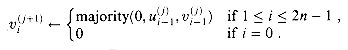
29-1 Division circuits
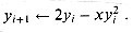
We can construct a division circuit from subtraction and multiplication circuits with a technique called Newton iteration. We shall focus on the related problem of computing a reciprocal, since we can obtain a division circuit by making one additional multiplication.
The idea is to compute a sequence y0, ,y1, y2, . . . of approximations to the reciprocal of a number x by using the formula
Assume that x is given as an n-bit binary fraction in the range 1/2
a. Suppose that
b. Give an initial approximation y0 such that yk satisfies
c. Describe a combinational circuit that, given an n-bit input x, computes an n-bit approximation to 1/x in O(lg2 n) time. What is the size of your circuit? (Hint: With a little cleverness, you can beat the size bound of
29-2 Boolean formulas for symmetric functions
A n-input function
for any permutation
a. We start by considering a simple symmetric function. The generalized majority function on n boolean inputs is defined by
Describe an O(lg n)-depth combinational circuit for majorityn. (Hint: Build a tree of adders.)
b. Suppose that
c. Argue that any symmetric boolean function f(x1, x2, . . . , xn ) can be expressed as a function of
d. Argue that any symmetric function on n boolean inputs can be computed by an O(lg n)-depth combinational circuit.
e. Argue that any symmetric boolean function on n boolean variables can be represented by a boolean formula whose length is polynomial in n.
Most books on computer arithmetic focus more on practical implementations of circuitry than on algorithmic theory. Savage [173] is one of the few that investigates algorithmic aspects of the subject. The more hardware-oriented books on computer arithmetic by Cavanagh [39] and Hwang [108] are especially readable. Good books on combinational and sequential logic design include Hill and Peterson [96] and, with a twist toward formal language theory, Kohavi [126].
Aiken and Hopper [7] trace the early history of arithmetic algorithms. Ripple-carry addition is as at least as old as the abacus, which has been around for over 5000 years. The first mechanical calculator employing ripple-carry addition was devised by B. Pascal in 1642. A calculating machine adapted to repeated addition for multiplication was conceived by S. Morland in 1666 and independently by G. W. Leibnitz in 1671. The Russian peasant's algorithm for multiplication is apparently much older than its use in Russia in the nineteenth century. According to Knuth [122], it was used by Egyptian mathematicians as long ago as 1800 B.C.
The kill, generate, and propagate statuses of a carry chain were exploited in a relay calculator built at Harvard during the mid-1940's [180]. One of the first implementations of carry-lookahead addition was described by Weinberger and Smith [199], but their lookahead method requires large gates. Ofman [152] proved that n-bit numbers could be added in O(lg n) time using carry-lookahead addition with constant-size gates.
The idea of using carry-save addition to speed up multiplication is due to Estrin, Gilchrist, and Pomerene [64]. Atrubin [13] describes a linear-array multiplier of infinite length that can be used to multiply binary numbers of arbitrary length. The multiplier produces the nth bit of the product immediately upon receiving the nth bits of the inputs. The Wallace-tree multiplier is attributed to Wallace [197], but the idea was also independently discovered by Ofman [152].
Division algorithms date back to I. Newton, who around 1665 invented what has become known as Newton iteration. Problem 29-1 uses Newton iteration to construct a division circuit with
 (n) steps (although teachers usually do not emphasize the number of steps required).(n) is the best asymptotic time bound we can hope to achieve for adding two n-digit numbers. With circuits that operate in parallel, however, we can do better. In this chapter, we shall design circuits that can quickly perform addition and multiplication. (Subtraction is essentially the same as addition, and division is deferred to Problem 29-1.) We shall assume that all inputs are n-bit natural numbers, expressed in binary.(n) time, and the carry-lookahead adder, which takes only O(1g n) time. It also presents the carry-save adder, which can reduce the problem of summing three numbers to the problem of summing two numbers in (1) time. Section 29.3 introduces two combinational multipliers: the array multiplier, which takes (n) time, and the Wallace-tree multiplier, which requires only (1g n) time. Finally, Section 29.4 presents circuits with clocked storage elements (registers) and shows how hardware can be saved by reusing combinational circuitry.
29.1 Combinational circuits
Combinational elements
 to denote the NOT function,
  to denote the AND function,
  to denote the XOR function, and
  to denote the XOR function. Thus, for example, 0 1 = 1.
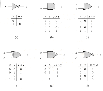
Figure 29.1 Six basic logic gates, with binary inputs and outputs. Under each gate is the truth table that describes the gate's operation. (a) The NOT gate. (b) The AND gate. (c) The OR gate. (d) The XOR (exclusive-OR) gate. (e) The NAND (NOT-AND) gate. (f) The NOR (NOT-OR) gate.
Combinational circuits
Full adders
x y z c s
-------------
0 0 0 0 0
0 0 1 0 1
0 1 0 0 1
0 1 1 1 0
1 0 0 0 1
1 0 1 1 0
1 1 0 1 0
1 1 1 1 1
s = parity(x,y,z) = x
y z,(29.1)
c = majority(x,y,z) = (x
y) (y z) (x z).(29.2)
 c, s
c, s = 10,1 which is the binary representation of 2, the sum of x, y, and z.
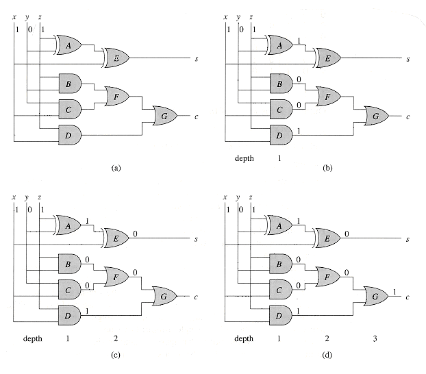
Figure 29.2 A full-adder circuit. (a) At time 0, the input bits shown appear on the three input wires. (b) At time 1, the values shown appear on the outputs of gates A-D, which are at depth 1. (c) At time 2, the values shown appear on the outputs of gates E and F, at depth 2. (d) At time 3, gate G produces its output, which is also the circuit output.
Circuit depth
Circuit size
Exercises
 lg n
lg n .
.29.2 Addition circuits
(n) time using a circuit with (n) size. This time bound can be improved to O(lg n) using a carry-lookahead adder, which also has (n) size. Finally, we present carry-save addition, which in O(1) time can reduce the sum of 3 n-bit numbers to the sum of an n-bit number and an (n + 1)-bit number. The circuit has (n) size.8 7 6 5 4 3 2 1 0 i
1 1 0 1 1 1 0 0 0 = c
0 1 0 1 1 1 1 0 = a
1 1 0 1 0 1 0 1 = b
-------------------------------
1 0 0 1 1 0 0 1 1 = s
Figure 29.3 Adding two 8-bit numbers a =
01011110 and b = 11010101 to produce a 9-bit sum s = 100110011. Each bit ci is a carry bit. Each column of bits represents, from top to bottom, ci, ai, bi, and si for some i. Carry-in c0 is always 0.29.2.1 Ripple-carry addition
an-1, an-2, . . . , a0, where n  lg(a + 1) and
 an-1, an-2, . . . , a0 and b = bn-1, bn-2, . . . , b0, we wish to produce an (n + 1)-bit sum s = sn, sn-1, . . . , s0. Figure 29.3 shows an example of adding two 8-bit numbers. We sum columns right to left, propagating any carry from column i to column i + 1, for i = 0, 1, . . . , n - 1. In the ith bit position, we take as inputs bits ai and bi and a carry-in bit ci, and we produce a sum bit si and a carry-out bit ci+1. The carry-out bit ci+1 from the ith position is the carry-in bit into the (i + 1)st position. Since there is no carry-in for position 0, we assume that c0 = 0. The carry-out cn is bit sn of the sum.sn, sn-1, . . . , s0, where sn equals cn, the carry-out bit from full adder FAn.(n). More precisely, full adder FAi is at depth i + 1 in the circuit. Because FAn-1 is at the largest depth of any full adder in the circuit, the depth of the ripple-carry adder is n. The size of the circuit is (n) because it contains n combinational elements.
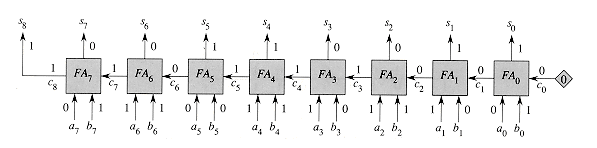
Figure 29.4 An 8-bit ripple-carry adder performing the addition of Figure 29.3. Carry bit c0 is hardwired to 0, indicated by the diamond, and carry bits ripple from right to left.
29.2.2 Carry-lookahead addition
(n) time because of the rippling of carry bits through the circuit. Carry-lookahead addition avoids this (n)-time delay by accelerating the computation of carries using a treelike circuit. A carry-lookahead adder can sum two n-bit numbers in O(lg n) time. 1, full adder FAi has two of its input values, namely ai and bi, ready long before the carry-in ci is ready. The idea behind the carry-lookahead adder is to exploit this partial information. bi-1, however, then ci depends on ci-1. Specifically, ci = ci-1, because the carry-in ci-1 casts the deciding "vote" in the majority election that determines ci. In this case, we propagate the carry, since the carry-out is the carry-in.
 over the domain {k, p, g}. An important property of this operator is that it is associative, as Exercise 29.2-2 asks you to verify.
ai-1 bi-1 ci carry status
-----------------------------
0 0 0 k
0 1 ci-1 p
1 0 ci-1 p
1 1 1 g
Figure 29.5 The carry-out bit ci and carry status corresponding to inputs ai-1, bi-1, and ci-1 of full adder FAi-1 in ripple-carry addition.
FAi
k p g--------------------
k k k g
FAi-1 p k p g
g k g g
Figure 29.6 The carry status of the combination of full adders FAi-1 and FAi in terms of their individual carry statuses, given by the carry-status operator
over the domain {k, p, g}.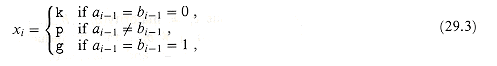
(29.3)
yi = yi-1
xi= x0
x1  xi
xi(29.4)
x1 xn; we call the process of computing the values y0, y1, . . . , yn a prefix computation. (Chapter 30 discusses prefix computations in a more general parallel context.) Figure 29.7 shows the values of xi and yi corresponding to the binary addition shown in Figure 29.3. The following lemma gives the significance of the yi values for carry-lookahead addition.
Figure 29.7 The values of xi and yi for i = 0, 1, . . . , 8 that correspond to the values of ai, bi, and ci in the binary-addition problem of Figure 29.3. Each value of xi is shaded with the values of ai-1 and bi-1 that it depends on.
xi, the definition of the carry-status operator from Figure 29.6 implies either that xi = k or that xi = p and yi-1 = k. If xi = k, then equation (29.3) implies that ai-1 = bi-1 = 0, and thus ci = majority (ai-1, bi-1, ci-1) = 0. If xi = p and yi-1 = k, then ai-1 bi-1 and, by induction, ci-1 = 0. Thus, majority (ai-1, bi-1, ci-1) = 0, and thus ci = 0. bi-1 and, by induction, ci-1 = 1, which implies ci= 1.(1) time by computing in parallel the sum bits si = parity (ai, bi, ci) for i = 0, 1, . . . , n (taking an = bn = 0). Thus, the problem of quickly adding two numbers reduces to the prefix computation of the carry statuses y0, y1, . . . ,yn.Computing carry statuses with a parallel prefix circuit
(n) size--asymptotically the same amount of hardware as a ripple-carry adder. i j n, we define
[i,j] = xi
xi+1 xj. i < j k n, we also have the identity[i,k] = [i,j - 1]
[j,k],(29.5)
operator. Figure 29.8 shows how pairs of elements are organized to form the internal nodes of a complete binary tree, and Figure 29.9 illustrates the parallel prefix circuit for n = 8. Note that the wires in the circuit follow the structure of a tree, but the circuit itself is not a tree, although it is purely combinational. The inputs x1, x2, . . . , xn are supplied at the leaves, and the input x0 is provided at the root. The outputs y0, y1, . . . , yn - 1 are produced at leaves, and the output yn is produced at the root. (For ease in understanding the prefix computation, variable indices increase from left to right in Figures 29.8 and 29.9, rather than from right to left as in other figures of this section.) elements in each node typically operate at different times and have different depths in the circuit. As shown in Figure 29.8, if the subtree rooted at a given node spans some range xi, xi+1, . . . , xk of inputs, its left subtree spans the range xi, xi+1, . . . , xj - 1, and its right subtree spans the range xj, xj+1, . . . , xk, then the node must produce for its parent the product [i, k] of all inputs spanned by its subtree. Since we can assume inductively that the node's left and right children produce the products [i, j - 1] and [j, k], the node simply uses one of its two elements to compute [i, k]  [i, j - 1] [j, k]. [0, i - 1] [i, k] and sends this value to the right child.
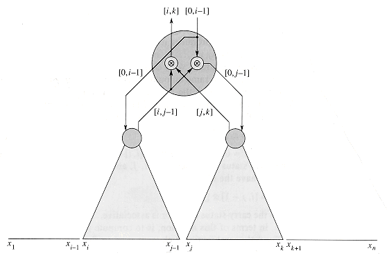
Figure 29.8 The organization of a parallel prefix circuit. The node shown is the root of a subtree whose leaves input the values xi to xk. The node's left subtree spans inputs xi to xj - 1, and its right subtree spans inputs xj to xk. The node consists of two
elements, which operate at different times during the operation of the circuit. One element computes [i, k] [i, j - 1] [j, k], and the other element computes [0, j - 1] [0, i - 1] [i, j - 1]. The values computed are shown on the wires. element is used to compute (in general) the value yn = [0, n] = [0, 0] [1, n]. elements. It takes only O(lg n) time to compute all n + 1 prefixes, since the computation proceeds up the tree and then back down. Exercise 29.2-5 studies the depth of the circuit in more detail.Completing the carry-lookahead adder
(1) size, and a parallel prefix circuit with inputs x0, x1, . . . , xn (x0 is hardwired to k) and outputs y0, y1, . . . , yn. KPG box KPGi takes external inputs ai and bi and produces sum bit si. (Input bits an and bn are hardwired to 0.) Given ai-1 and bi-1, box KPGi-1 computes xi  {k,p,g} according to equation (29.3) and sends this value as the external input xi of the parallel prefix circuit. (The value of xn+1 is ignored.) Computing all the xi takes (1) time. After a delay of O(lg n), the parallel prefix circuit produces y0, y1, . . . , yn. By Lemma 29.1, yi is either k or g; it cannot be p. Each value yi indicates the carry-in to full adder FAi in the ripple-carry adder: yi = k implies ci = 0, and yi = g implies ci = 1. Thus, the value of yi is fed into KPGi to indicate the carry-in ci, and the sum bit si = parity(ai, bi, ci) is produced in constant time. Thus, the carry-lookahead adder operates in O(lg n) time and has (n) size.
Figure 29.9 A parallel prefix circuit for n = 8. (a) The overall structure of the circuit, and the values carried on each wire. (b) The same circuit with values corresponding to Figures 29.3 and 29.7.
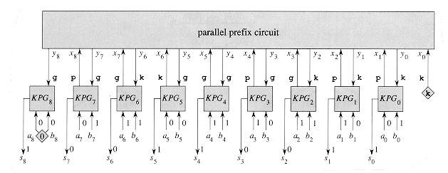
Figure 29.10 The construction of an n-bit carry-lookahead adder, shown here for n = 8. It consists of n + 1 KPG boxes KPGi for i = 0, 1, . . . , n. Each box KPGi takes external inputs ai and bi (where an and bn are hardwired to 0, as indicated by the diamond) and computes carry status xi+1. These values are fed into the parallel prefix circuit, which returns the results yi of the prefix computation. Each box KPGi now takes yi as input, interprets it as the carry-in bit ci, and then outputs the sum bit si = parity (ai, bi, ci). Sample values corresponding to those shown in Figures 29.3 and 29.9 are shown.
29.2.3 Carry-save addition
xn-1, xn-2, . . . . , x0, y = yn-1, yn-2, . . . , y0, and z = zn-1,zn-2, . . . , z0, an n-bit carry-save adder produces an n-bit number u = un-1, un-2, . . . , u0 and an (n + 1)-bit number v = vn, vn-1, . . . , v0 such thatu + v = x + y + z.
ui = parity (xi, yi, zi),
vi + 1 = majority (xi, yi, zi),
(1) time and has (n) size. To sum three n-bit numbers, therefore, we need only perform a carry-save addition, taking (1) time, and then perform a carry-lookahead addition, taking O(lg n) time. Although this method is not asymptotically better than the method of using two carry-lookahead additions, it is much faster in practice. Moreover, we shall see in Section 29.3 that carry-save addition is central to fast algorithms for multiplication.
Figure 29.11 (a) Carry-save addition. Given three n-bit numbers x, y, and z, we produce an n-bit number u and an (n + 1)-bit number v such that x + y + z = u + v. The ith pair of shaded bits are a function of xi, yi, and zi. (b) An 8-bit carry-save adder. Each full adder FAi takes inputs xi, yi, and zi and produces sum bit ui and carry-out bit vi + 1. Bit v0 is hardwired to 0.
Exercises
01111111, b = 00000001, and n = 8. Show the sum and carry bits output by full adders when ripple-carry addition is performed on these two sequences. Show the carry statuses x0, x1, . . . , x8 corresponding to a and b, label each wire of the parallel prefix circuit of Figure 29.9 with the value it has given these xi inputs, and show the resulting outputs y0, y1, . . . , y8. given by Figure 29.5 is associative.
Figure 29.12 A parallel prefix circuit for use in Exercise 29.2-6.
00 if xi = k, by 11 if xi = g, and by 01 or 10 if xi = p. Assume also that each input yi is represented by 0 if yi = k and by 1 if yi = g. elements that operate (lg n) time apart. Is there a node whose elements operate simultaneously?(lg n) and that it has (n lg n) size.(n)-size circuit even if we restrict gates to have O(1) fan-out.lg(n + 1) outputs. Interpreted as a binary number, the outputs give the number of 1's in the inputs. For example, if the input is 10011110, the output is 101, indicating that there are five 1's in the input. Describe an O(lg n)-depth tally circuit having (n) size.(n), for two random numbers, the outputs almost always settle within O(lg n) time.29.3 Multiplication circuits
p2n-1, p2n-2, . . . . , p0 of two n-bit numbers a = an-1, an-2, . . . , a0 and b = bn-1, bn-2, . . . , b0. We examine the bits of b, from b0 up to bn-1. For each bit bi with a value of 1, we add a into the product, but shifted left by i positions. For each bit bi with a value of 0, we add in 0. Thus, letting m(i) = a . bi . 2i, we compute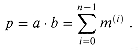 (n) time and have (n2) size. Wallace-tree multipliers also have (n2) size, but they operate in (lg n) time. Both circuits are based on the grade-school algorithm.
 1 1 1 0 = a
1 1 0 1 = b
-------------------------------
1 1 1 0 = m(0)
0 0 0 0 = m(1)
1 1 1 0 = m(2)
1 1 1 0 = m(3)
-------------------------------
1 0 1 1 0 1 1 0 = p
Figure 29.13 The "grade-school" multiplication method, shown here multiplying a =
1110 by b = 1101 to obtain the product p = 10110110. We add  , where m(i) = a bi 2i. Here, n = 8. Each term m(i) is formed by shifting either a (if bi = 1 ) or 0 (if bi = 0) i positions to the left. Bits that are not shown are 0 regardless of the values of a and b.
29.3.1 Array multipliers
an-1, an-2, . . . , a0 and b = bn-1, bn-2, . . . , b0. The aj values run vertically, and the bi values run horizontally. Each input bit fans out to n AND gates to form partial products. Full adders, which are organized as carry-save adders, sum partial products. The lower-order bits of the final product are output on the right. The higher-order bits are formed by adding the two numbers output by the last carry-save adder.an-1, an-2, . . . , a0 and b = bn-1, bn-2, . . . , b0, the bits of the partial products are easy to compute. Specifically, for i, j = 0, 1, . . . , n - 1, we have
 and
and  are 0.) We then have m(0) + m(1) + m(2) = u(2) + v(2). The multiplier continues on, carry-save adding u(i-1), v(i-1), and m(i) for i = 2, 3, . . . , n - 1. The result is a (2n - 1)-bit number u(n - l) and a (2n - 1)-bit number v(n - 1), where
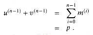
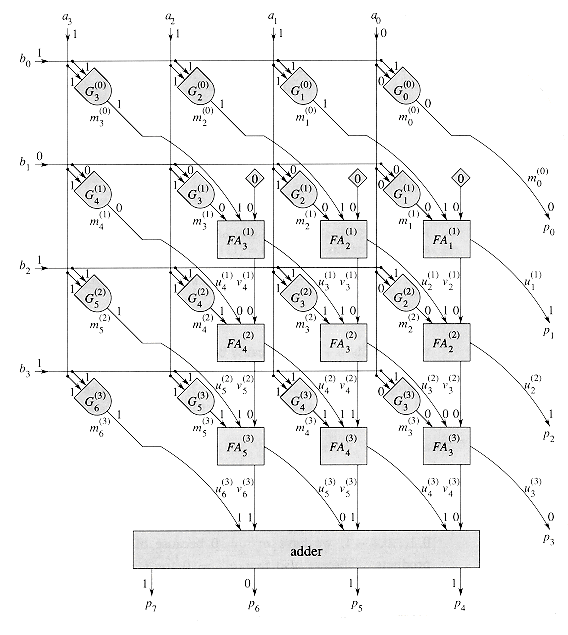
Figure 29.14 An array multiplier that computes the product p =
p2n-1,p2n-2, . . . , p0 of two n-bit numbers a = an-1,an-2, . . . ,a0 and b = bn-1,bn-2, . . . , b0, shown here for n = 4. Each AND gate  computes partial-product bit
  . Each row of full adders constitutes a carry-save adder. The lower n bits of the product are
  and the u bits coming out from the rightmost column of full adders. The upper n product bits are formed by adding the u and v bits coming out from the bottom row of full adders. Shown are bit values for inputs a = 1110 and b = 1101 and product p = 10110110, corresponding to Figures 29.13 and 29.15.
 0 0 0 0 = 0
1 1 1 0 = m(0)
0 0 0 0 = m(1)
-------------------------------
0 1 1 1 0 = u(1)
0 0 0 = v(1)
1 1 1 0 = m(2)
-------------------------------
1 1 0 1 1 0 = u(2)
0 1 0 = v(2)
1 1 1 0 = m(3)
-------------------------------
1 0 1 0 1 1 0 = u(3)
1 1 0 = v(3)
-------------------------------
1 0 1 1 0 1 1 0 = p
Figure 29.15 Evaluating the sum of the partial products by repeated carry-save addition. For this example, a =
1110 and b = 1101 . Bits that are blank are 0 regardless of the values of a and b. We first evaluate m(0) + m(1) + 0 = u(1) + v(1) then u(1) + v(1)+ m(2) = u(2) + v(2), then u(2) + v(2) + m(3) = u(3) + v(3), and finally p = m(0) + m(1) + m(2) + m(3) = u(3) + v(3) Note that  and
and  for i = 1, 2, . . . , n - 1.
 because of how we shift the partial products. Observe also that
  for i = 1, 2, . . . , n - 1 and j = 0, 1, . . . , i, i + n, i + n + 1, . . . , 2n - 1. (See Exercise 29.3-1.) Each carry-save addition, therefore, needs to operate on only n - 1 bits.
 for some i and j in the ranges 0 i n - 1 and 0 j 2n - 2. Gate
  produces
  , the jth bit of the ith partial product. For i = 0, 1, . . . , n - 1, the ith row of AND gates computes the n significant bits of the partial product m(i), that is,
  .
. takes three input
  , and
, and  --and produces two output
  and
and  . (Note that in the leftmost column of full adders,
  .) Each full adder
  in the top row takes inputs
  , and 0 and produces bits
  .
. for j = 0, 1, . . . , n - 1. Thus,
  for j = 0, 1, . . . , n - 1. Moreover, since
  , we have
  , and since the lowest-order i bits of each m(i) and v(i - 1) are 0, we have
  for i = 2, 3, . . . , n- 1 and j = 0, 1, . . . , i - 1. Thus,
  and, by induction,
  for i = 1, 2, . . . , n - 1. Product bitsp2n-1, p2n-2, . . . , pn are produced by an n-bit adder that adds the outputs from the last row of full adders:
Analysis
(n) time for the lower-order product bits pn-1, pn-2, . . . , p0 to be produced, and it takes (n) time for the inputs to the adder to be ready. If the adder is a ripple-carry adder, it takes another (n) time for the higher-order product bits p2n-1, p2n-2, . . . , pn to emerge. If the adder is a carry-lookahead adder, only (lg n) time is needed, but the total time remains (n).(n) gates. Thus, the array multiplier has (n2) size.29.3.2 Wallace-tree multipliers
(n)-bit numbers. It does this by using  n/3
n/3 carry-save adders in parallel to convert the sum of n numbers to the sum of 2n/3 numbers. It then recursively constructs a Wallace tree on the 2n/3 resulting numbers. In this way, the set of numbers is progressively reduced until there are only two numbers left. By performing many carry-save additions in parallel, Wallace trees allow two n-bit numbers to be multiplied in (1g n) time using a circuit with (n2) size.
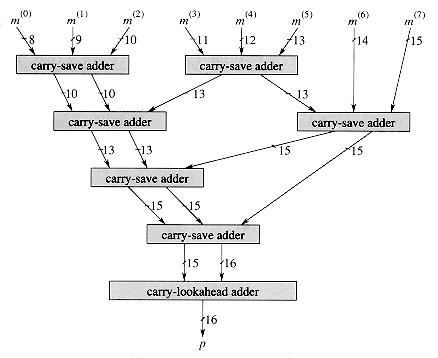
Figure 29.16 A Wallace tree that adds n = 8 partial products m(0), m(1), . . . , m(7). Each line represents a number with the number of bits indicated. The left output of each carry-save adder represents the sum bits, and the right output represents the carry bits.
Analysis
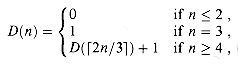 (1g n) by case 2 of the master theorem (Theorem 4.1). Each carry-save adder takes (1) time. All n partial products can be formed in (1) time in parallel. (The lowest-order i - 1 bits of m(i), for i = 1, 2, . . . , n - 1, are hardwired to 0.) The carry-lookahead adder takes O(lg n) time. Thus, the entire multiplication of two n-bit numbers takes (lg n) time.(n2) size, which we can see as follows. We first bound the circuit size of the carry-save adders. A lower bound of
  (n2) is easy to obtain, since there are 2n/3 carry-save adders at depth 1, and each one consists of at least n full adders. To get the upper bound of O(n2), observe that since the final product has 2n bits, each carry-save adder in the Wallace tree contains at most 2n full adders. We need to show that there are O(n) carry-save adders altogether. Let C(n) be the total number of carry-save adders in a Wallace tree with n input numbers. We have the recurrence
 (n) by case 3 of the master theorem. We thus obtain an asymptotically tight bound of (n2) size for the carry-save adders of a Wallace-tree multiplier. The circuitry to set up the n partial products has (n2) size, and the carry-lookahead adder at the end has (n) size. Thus, the size of the entire multiplier is (n2).
Exercises
 = 0 for i = 1, 2, . . . , n - 1 and j = 0, 1,. . . , i, i + n, i + n + 1, . . . , 2n - 1. ny nz. Show that ns= nz and that
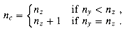 .xn-1, xn-2,. . . ,x0 and s = sm-1, sm-2,. . . , s0, where m = lg n. Its output y = yn-1, yn-2,. . . , y0 is specified by yi = xi + smodn, for i = 0,1, . . ., n - 1. That is, the shifter rotates the bits of x by the amount specified by s. Describe an efficient cyclic shifter. In terms of modular multiplication, what function does a cyclic shifter implement?
29.4 Clocked circuits
(1)-size clocked circuit, called a bit-serial adder, that can add two n-bit numbers in (n) time. We then investigate linear-array multipliers. We present a linear-array multiplier with (n) size that can multiply two n-bit numbers in (n) time.29.4.1 Bit-serial addition
sn, sn - 1, . . . , s0 of two n-bit numbers a = an - 1, an - 2, . . . , a0 and b = bn - 1, bn - 2, . . . , b0. The external world presents the input bits one pair at a time: first a0 and b0, then a1 and b1, and so forth. Although we want the carry-out from one bit position to be the carry-in to the next bit position, we cannot just feed the full adder's c output directly into an input. There is a timing issue: the carry-in ci entering the full adder must correspond to the appropriate inputs ai and bi. Unless these input bits arrive at exactly the same moment as the fed-back carry, the output may be incorrect.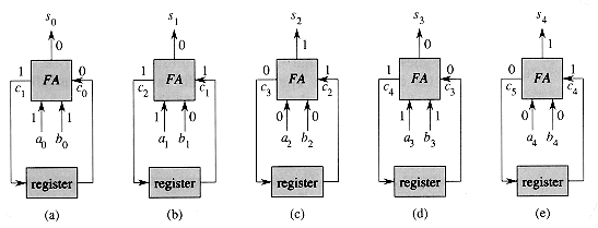
Figure 29.17 The operation of a bit-serial adder. During the ith clock period, for i = 0, 1, . . . , n, the full adder FA takes input bits ai and bi from the outside world and a carry bit ci from the register. The full adder then outputs sum bit si, which is provided externally, and carry bit ci+1, which is stored back in the register to be used during the next clock period. The register is initialized with c0 = 0. (a)-(e) The state of the circuit in each of the five clock periods during the addition of a =
1011 and b = 1001 to produce s = 10100.Analysis
(1) time because the depth of the full adder is (1). Since n + 1 clock ticks are required to produce all the outputs, the total time to perform bit-serial addition is (n + 1) (1) = (n).(1).Ripple-carry addition versus bit-serial addition
(n) less for the bit-serial adder versus the ripple-carry adder), but the combinational circuit has the advantage of less control circuitry--we need no clock or synchronized external circuit to present input bits and store sum bits. Moreover, although the circuits have the same asymptotic time delay, the combinational circuit typically runs slightly faster in practice. The extra speed is possible because the combinational circuit doesn't have to wait for values to stabilize during each clock period. If all the inputs stabilize at once, values just ripple through the circuit at the maximum possible speed, without waiting for the clock.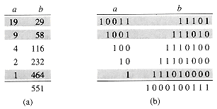
Figure 29.18 Multiplying 19 by 29 with the Russian peasant's algorithm. The a- column entry in each row is half of the previous row's entry with fractions ignored, and the b-column entries double from row to row. We add the b-column entries in all rows with odd a-column entries, which are shaded. This sum is the desired product. (a) The numbers expressed in decimal. (b) The same numbers in binary.
29.4.2 Linear-array multipliers
(n2) size to multiply two n-bit numbers. We now present two multipliers that are linear, rather than two-dimensional, arrays of circuit elements. Like the array multiplier, the faster of these two linear-array multipliers runs in (n) time. b.A slow linear-array implementation
 , and we define
 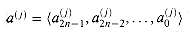 .
.a(j)
b(j) + p(j) = a b(29.6)
 ), then add b into p: p(j+1) b(j) + p(j). (The addition is performed by a ripple-carry adder that runs the length of the array; carry bits ripple from right to left.) If a(j) is even, then carry p through to the next step: p(j+1) p(j).
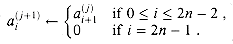
 b.(n) time in the worst case, because the depth of the ripple-carry adder is (n), and thus the duration of the clock period must be at least (n). Each shift takes only (1) time. Overall, therefore, the algorithm takes (n2) time. Because each cell has constant size, the entire linear array has (n) size.
A fast linear-array implementation
(1), thus improving the overall time to (n). As Figure 29.19(b) shows, once again each cell contains a bit of an a entry and a bit of a b entry. Each cell also contains two more bits, from u and v, which are the outputs from carry-save addition. Using a carry-save representation to accumulate the product, we maintain the invariant that before the jth step,a(j)
b(j) + u(j) + v(j) = a b(29.7)
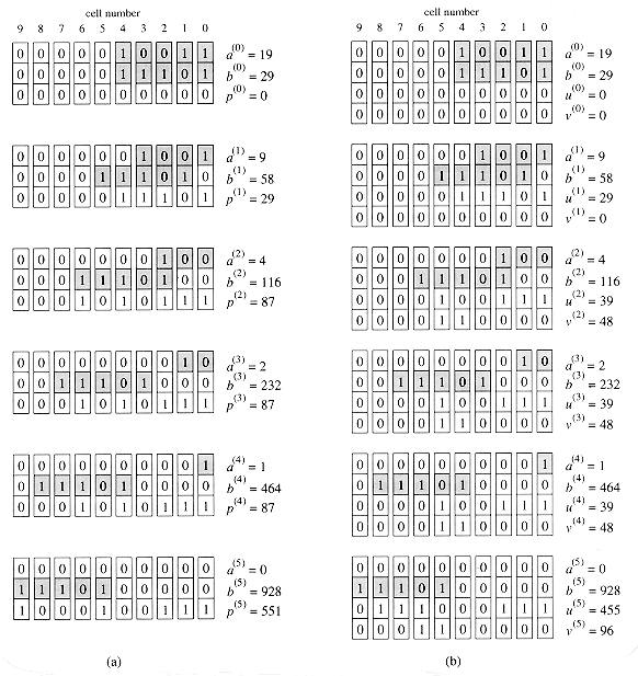
Figure 29.19 Two linear-array implementations of the Russian peasant's algorithm, showing the multiplication of a = 19 =
10011 by b = 29 = 11101, with n = 5. The situation at the beginning of each step j is shown, with the remaining significant bits of a(j) and b(j) shaded. (a) A slow implementation that runs in (n2) time. Because a(5) = 0, we have p(5) = a b. There are n steps, and each step uses a ripple-carry addition. The clock period is therefore proportional to the length of the array, or (n), leading to (n2) time overall. (b) A fast implementation that runs in (n) time because each step uses carry-save addition rather than ripple-carry addition, thus taking only (1) time. There are a total of 2n - 1 = 9 steps; after the last step shown, repeated carry-save addition of u and v yields u(9) = a b. , we compute
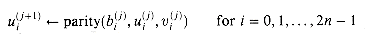
 , and we compute
 n, we have a(j) = 0, and invariant (29.7) therefore implies that u(j) + v(j) = a b. Once a(j) = 0, all further steps serve only to carry-save add u and v. Exercise 29.4-3 asks you to show that v(2n-1) = 0, so that u(2n-1) = a b.(n), since each of the 2n - 1 steps takes (1) time. Because each cell still has constant size, the total size remains (n).
Exercises
101101, b = 011110, and n = 6. Show how the Russian peasant's algorithm operates, in both decimal and binary, for inputs a and b.x1, x2, . . . that arrives at a clocked circuit at the rate of 1 value per clock tick. For a fixed value n, the circuit must compute the value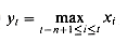
Problems
 x 1. Since the reciprocal can be an infinite repeating fraction, we shall concentrate on computing an n-bit approximation accurate up to its least significant bit.
 yi - 1/x for some constant > 0. Prove that yi+1 - 1/x 2. yk - 1/x 2-2k for all k 0. How large must k be for the approximation yk to be accurate up to its least significant bit?(n2 lgn).)
 (x1, x2, . . . , xn) is symmetric if
f(x1, x2, . . . , xn) =
(x (1), x(2), . . . , x(n) ) of {1,2, . . . , n}. In this problem, we shall show that there is a boolean formula representing whose size is polynomial in n. (For our purposes, a boolean formula is a string comprised of the variables x1, x2, . . . , xn, parentheses, and the boolean operators V,
  , and .) Our approach will be to convert a logarithmic-depth boolean circuit to an equivalent polynomial-size boolean formula. We shall assume that all circuits are constructed from 2-input AND, 2-input OR, and NOT gates.
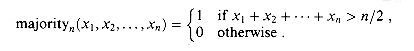 is an arbitrary boolean function of the n boolean variables x1, x2, . . . , xn. Suppose further that there is a circuit C of depth d that computes . Show how to construct from C a boolean formula for of length O(2d). Conclude that there is polynomial-size formula for majorityn.
Chapter notes
(lg2 n) depth. This method was improved by Beame, Cook, and Hoover [19], who showed that n-bit division can in fact be performed in (lg n) depth.